
The EpiNex® Process
A Smarter Way to Make Silicon Wafers.
EpiNex® grows precision-engineered silicon wafers directly from gas, eliminating conventional ingot growth and wire sawing. The process enables precise control of wafer thickness and doping profiles while dramatically improving silicon utilization.
Seed. Grow. Release.
Direct gas-to-wafer manufacturing process
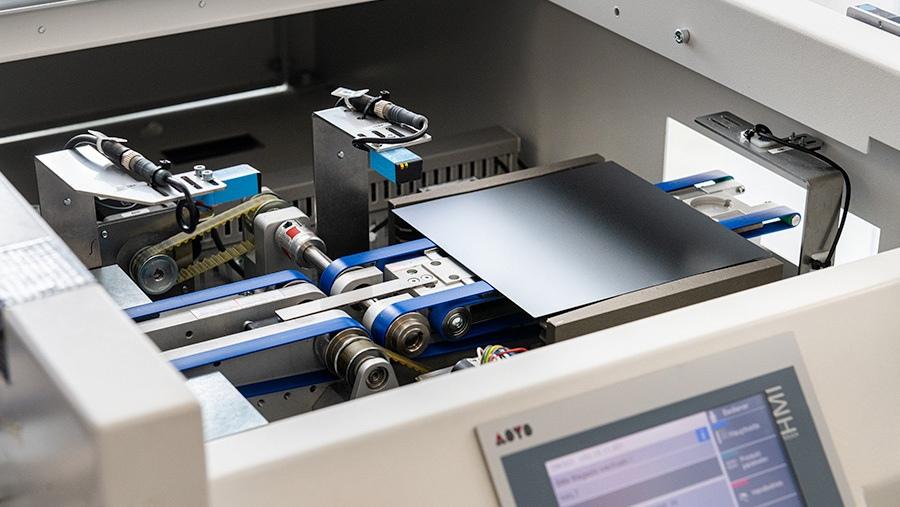
01 / Seed
Prepare a reusable silicon seed with a porous separation layer.
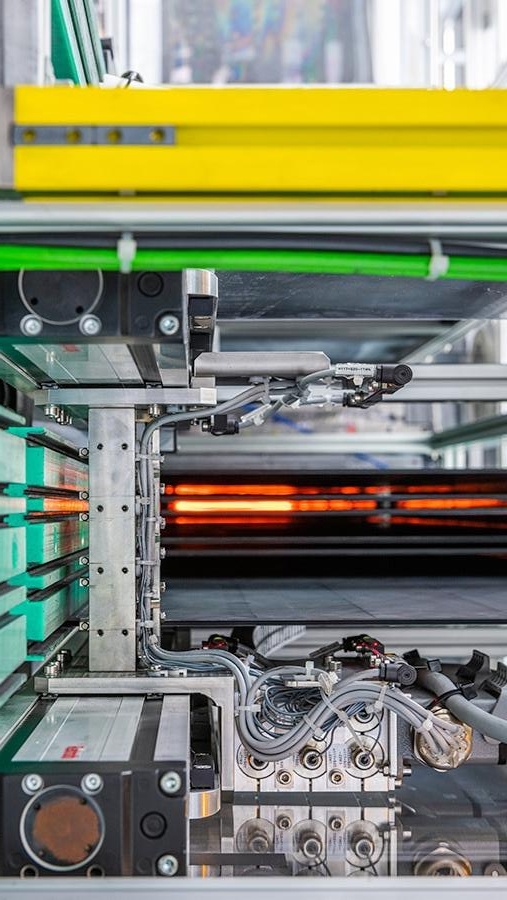
02 / Grow
Grow the wafer epitaxially, precisely controlling thickness and doping profiles.
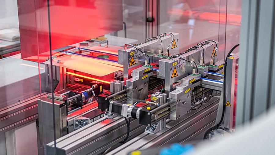
03 / Release
Separate the finished wafer and reclaim the seed for reuse.
Precision Engineering.
Built Into Every Wafer.
Ultra-Thin Precision & Uniformity
Precise thickness and resistivity control at ultra-thin dimensions, supporting tighter efficiency distributions.
Engineered Doping for Radiation Resilience
Precisely controlled boron doping gradients create internal electric fields that reduce radiation-induced power loss.
Low Oxygen. No Gallium Dependency.
Ultra-low oxygen content reduces the risk of boron–oxygen degradation, without gallium doping.
Silicon utilization
Precision-Grown. Not Cut from an Ingot.
EpiNex® wafers are grown directly to their required thickness, rather than sliced from an ingot. This eliminates conventional wire-saw kerf losses.
The Thinner the Wafer, the Greater the Silicon Savings
As wafer thickness decreases, conventional slicing losses account for an increasing share of silicon consumption. Additional thinning processes can further increase these losses.
Efficiency = finished wafer silicon ÷ (finished wafer silicon + non-recoverable loss)
EpiNex® 80%
CZ wafer 44%
1.8× more silicon used with EpiNex at this thickness
Methodology
Material-loss values are process-model assumptions, not measured production data.
- Silicon utilization = finished-wafer silicon ÷ (finished-wafer silicon + non-recoverable silicon loss).
- EpiNex®: modeled non-recoverable silicon loss of 17 µm per wafer, associated with the reusable seed process.
- CZ: modeled slicing loss of 59 µm per wafer, plus additional thinning from 100 µm for wafers thinner than 100 µm.
Source: NexWafe internal analysis.
Contact us
Ready to explore your options?
Contact our team at . Our team is here to help.