01 / Demonstrated Performance
Superior Radiation Resilience
Higher efficiency retention demonstrated in electron and proton irradiation tests.
>9% improvement in efficiency retention at EOL vs CZ
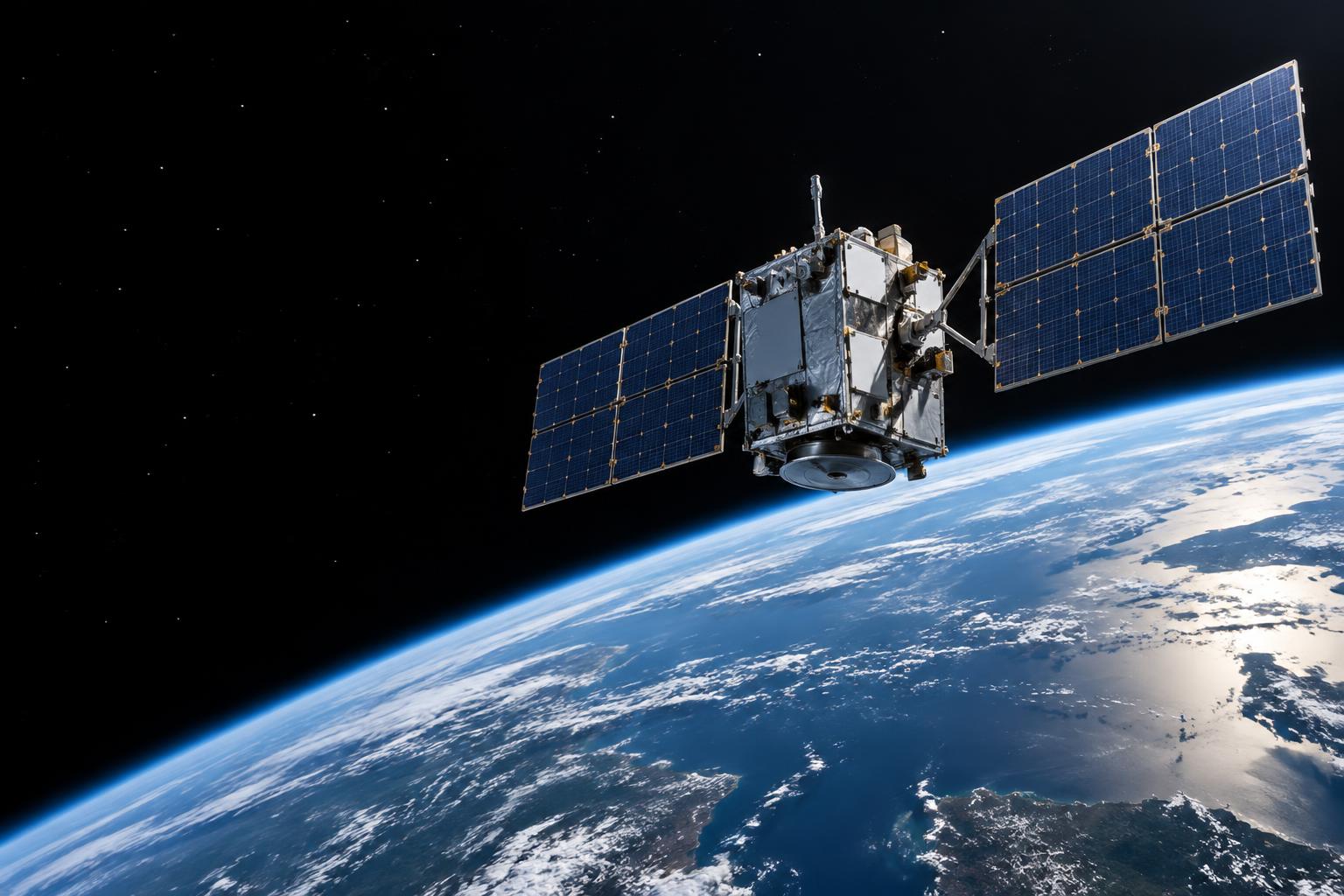

EpiNex® for space
Engineered silicon wafers for PERC and HJT solar cells, delivering improved end-of-life power output for satellites and thin, high-efficiency solutions for HAPS.
Radiation Resilience
EpiNex® engineered silicon improves radiation resilience, giving satellite designers greater flexibility to optimize solar array size, mass and end-of-life power.
01 / Demonstrated Performance
Higher efficiency retention demonstrated in electron and proton irradiation tests.
>9% improvement in efficiency retention at EOL vs CZ
02 / System Advantage
Maintain required end-of-life power with less array mass and potentially lower drag.
03 / Mission Value
Extended Power Availability
Maintain required solar power for longer with the same array size.
The Case for Silicon in Space

High conversion efficiency, limited manufacturing scale, and high costs constrain deployment at the scale needed for larger LEO constellations.
Engineered EpiNex® wafers enable radiation-resilient silicon solar cells using established, high-volume cell manufacturing technologies.
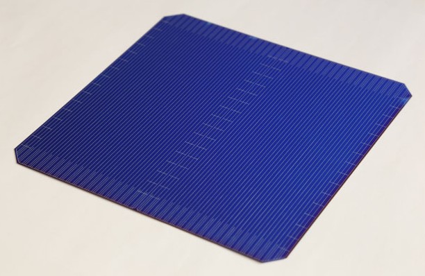
The EpiNex® process
Direct Gas-to-Wafer Technology
EpiNex® grows precision-engineered silicon wafers directly from gas, eliminating conventional ingot growth and wire sawing. Precise control of doping profiles during growth enables improved radiation resilience and solar cell performance while using silicon more efficiently.
A reusable silicon seed wafer is prepared with an engineered porous separation layer.
Silicon is grown directly to final thickness with precisely controlled doping profiles.
The finished wafer is detached, and the seed is reclaimed for reuse.
Strategic Supply
Building a resilient Western wafer supply chain for next-generation solar power.
Silicon is designated a U.S. critical mineral.
No reliance on gallium as the wafer dopant.
Western production and supply chains without critical dependencies.
Engineering the Future of Space Power
Explore how NexWafe is building the manufacturing capacity to bring engineered silicon wafers to scale.