
EpiNex® Engineered Wafers
Engineered Silicon.
More Power for Longer.
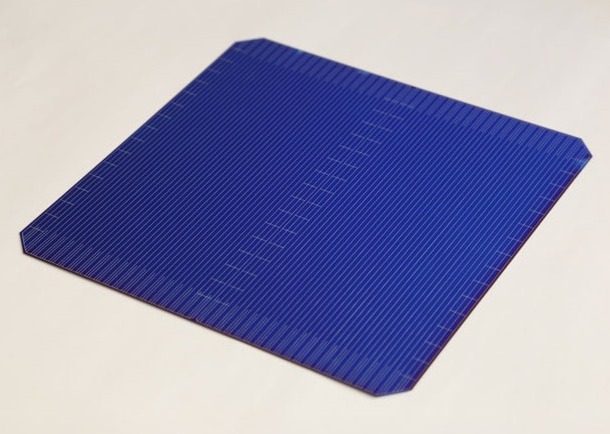
Ultra-thin silicon wafers with engineered doping profiles designed to improve radiation resilience and preserve solar cell performance throughout a satellite mission.
01
Radiation Resilience
Improved efficiency retention demonstrated in electron and proton testing.
02
Smaller, Lighter Arrays. Longer Missions.
Improved radiation resilience can enable smaller, lighter solar arrays for a given end-of-life power requirement, or potentially extend mission life with the same array size.
03
Scalable Manufacturing
Direct gas-to-wafer production without conventional ingot growth or wire sawing.
Demonstrated radiation performance
Engineered Wafers. Higher End-of-Life Power.
Measured Cell Efficiency
Absolute solar cell efficiency before and after accelerated 5 MeV proton testing: engineered EpiNex® wafers versus conventional CZ silicon.
Engineered Doping Gradients Improve Radiation Resilience
Following accelerated 5 MeV proton testing, graded EpiNex® cells achieved 18.0% efficiency, compared with 16.8% for both uniformly doped CZ and EpiNex® controls.
Test context: Results are from experimental mini-cell coupons developed for comparative radiation testing, not optimized commercial-size solar cells. The relevant comparison is relative radiation-induced degradation and post-irradiation efficiency under identical test conditions.
Test conditions: 5 MeV protons, fluence 5 × 10⁹ p/cm². Efficiencies measured under AM1.5 illumination.
Degradation percentages represent relative efficiency loss from BOL.
How It Works
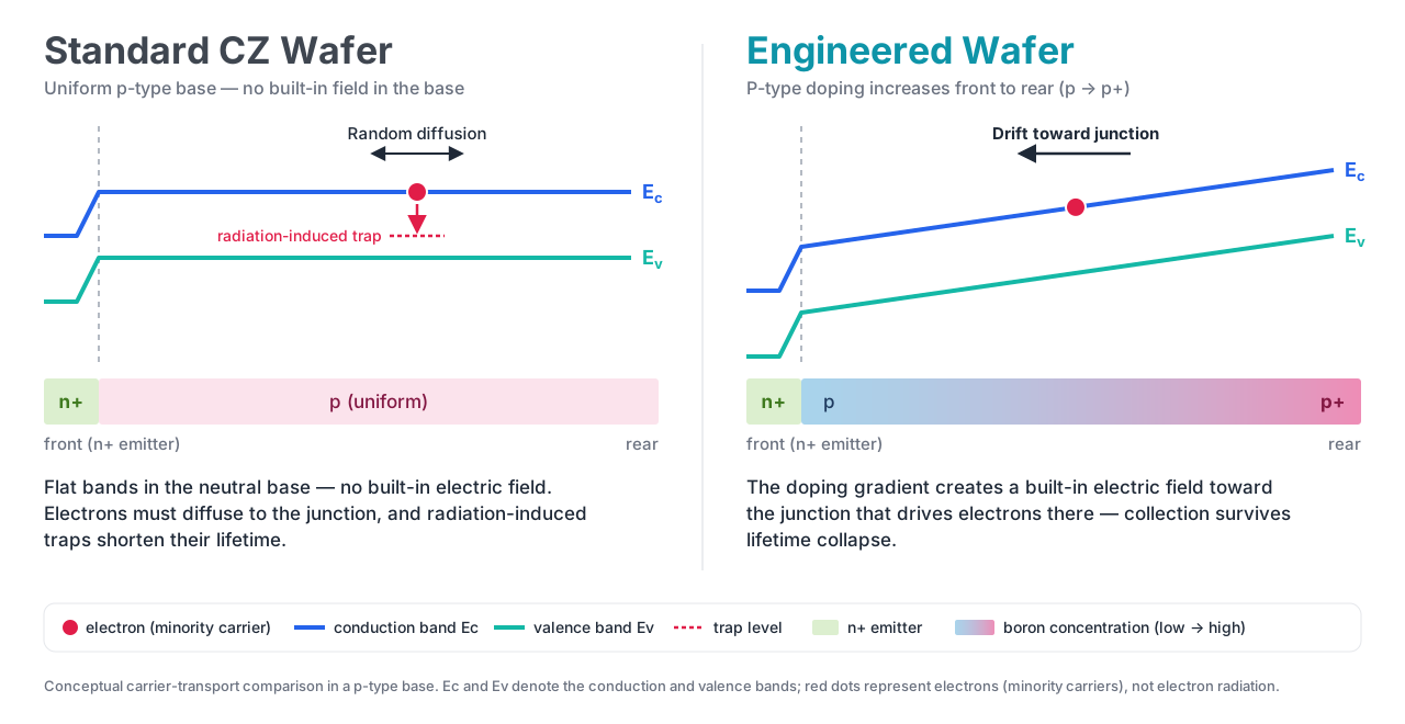
Engineered Electric Fields Reduce Radiation-Induced Power Loss
EpiNex® wafers incorporate precisely controlled boron doping gradients formed during epitaxial growth. These gradients create an internal electric field that assists minority-carrier electron transport toward the collecting junction, mitigating radiation-induced power degradation.

Contact us
Ready to explore your options?
Contact our team at . Our team is here to help.